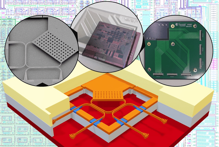

A team of researchers led by the University of Sydney’s Associate Professor Niels Quack has developed a new technology to combine optics and micro-electro mechanical systems (MEMS) in a microchip, paving the way for the creation of devices like micro-3D cameras and gas sensors for precision air quality measurement, including their use in mobile phones.
Published today in Nature: Microsystems and NanoEngineering, the new microfabrication process builds on silicon photonics and uses semiconductor manufacturing techniques to enable a new, more energy-efficient generation of devices for fibre-optical communications, sensors and even future quantum computers.
Associate Professor Quack from the School of Aerospace, Mechanical and Mechatronic Engineering said that the photonic MEMS are unique in that they are compact, consume very little power, are fast, support a broad range of optical carrier signals and have low optical loss.
“This is the first time that nano-electro-mechanical actuators have been integrated in a standard silicon photonics technology platform,” Associate Professor Quack said.
“It is an important step towards mature large-scale, reliable photonic circuits with integrated MEMS. This technology is being prepared for high-volume production, with potential applications in 3D imaging for autonomous vehicles or new photonic assisted computing.
“Current similar technologies consume a lot of power and occupy a large area on-chip. They also have high optical losses. This makes the integration of a large number of components on a single chip challenging,” he said.
“Our silicon photonic MEMS technology overcomes these shortcomings, providing a route for efficient scaling of photonic integrated circuits.
“The technology will advance knowledge in the field of micro- and nanofabrication, photonics and semiconductors, with a wide range of applications. These include beam steering for LIDAR 3D sensing in autonomous vehicles, programmable photonic chips, or information processing in quantum photonics.”
DECLARATION
The authors declare no competing interests. This work has been supported by the European Union through the H2020 project MORPHIC under grant 780283. N.Q. acknowledges funding by the Swiss National Science Foundation under grant 183717. The work reported in this manuscript was performed while N.Q. was at EPFL, and the manuscript was in part composed while N.Q. was at the University of Sydney. The authors acknowledge the support of the EPFL Center of MicroNanoTechnology (CMi).
DOI
10.1038/s41378-023-00498-z
Method of Research
Experimental study
Subject of Research
Not applicable
Article Title
Integrated silicon photonic MEMS
Article Publication Date
20-Mar-2023
COI Statement
The authors declare no competing interests. This work has been supported by the European Union through the H2020 project MORPHIC under grant 780283. N.Q. acknowledges funding by the Swiss National Science Foundation under grant 183717. The work reported in this manuscript was performed while N.Q. was at EPFL, and the manuscript was in part composed while N.Q. was at the University of Sydney. The authors acknowledge the support of the EPFL Center of MicroNanoTechnology (CMi).